- 您现在的位置:买卖IC网 > Sheet目录513 > SI7904BDN-T1-GE3 (Vishay Siliconix)MOSFET N-CH DL 20V PPAK 1212-8
�� �
�
�AN822�
�Vishay� Siliconix�
�PowerPAK� 1212� DUAL�
�To� take� the� advantage� of� the� dual� PowerPAK� 1212-8’s�
�thermal� performance,� the� minimum� recommended�
�land� pattern� can� be� found� in� Application� Note� 826,�
�Recommended Minimum Pad Patterns With Outline�
�Drawing Access for Vishay Siliconix MOSFETs� .� Click�
�on� the� PowerPAK� 1212-8� dual� in� the� index� of� this� doc-�
�ument.�
�The� gap� between� the� two� drain� pads� is� 10� mils.� This�
�matches� the� spacing� of� the� two� drain� pads� on� the� Pow-�
�erPAK� 1212-8� dual� package.�
�This� land� pattern� can� be� extended� to� the� left,� right,� and�
�top� of� the� drawn� pattern.� This� extension� will� serve� to�
�increase� the� heat� dissipation� by� decreasing� the� ther-�
�mal� resistance� from� the� foot� of� the� PowerPAK� to� the�
�PC� board� and� therefore� to� the� ambient.� Note� that�
�increasing� the� drain� land� area� beyond� a� certain� point�
�will� yield� little� decrease� in� foot-to-board� and� foot-to-�
�ambient� thermal� resistance.� Under� specific� conditions�
�of� board� configuration,� copper� weight,� and� layer� stack,�
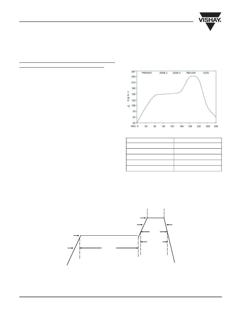
�ture� profile� used,� and� the� temperatures� and� time�
�duration,� are� shown� in� Figures� 2� and� 3.� For� the� lead�
�(Pb)-free� solder� profile,� see� http://www.vishay.com/�
�doc?73257.�
�experiments� have� found� that� adding� copper� beyond� an�
�area� of� about� 0.3� to� 0.5� in� 2� of� will� yield� little� improve-�
�ment� in� thermal� performance.�
�REFLOW� SOLDERING�
�Vishay� Siliconix� surface-mount� packages� meet� solder�
�Ramp-Up� Rate�
�Temperature� at� 155� ±� 15� °� C�
�Temperature� Above� 180� °� C�
�Maximum� Temperature�
�Time� at� Maximum� Temperature�
�Ramp-Down� Rate�
�+� 6� °� C� /Second� Maximum�
�120� Seconds� Maximum�
�70� -� 180� Seconds�
�240� +� 5/-� 0� °� C�
�20� -� 40� Seconds�
�+� 6� °� C/Second� Maximum�
�reflow� reliability� requirements.� Devices� are� subjected�
�to� solder� reflow� as� a� preconditioning� test� and� are� then�
�Figure� 2.� Solder� Reflow� Temperature� Profile�
�reliability-tested� using� temperature� cycle,� bias� humid-�
�ity,� HAST,� or� pressure� pot.� The� solder� reflow� tempera-�
�10� s� (max)�
�210� -� 220� °C�
�140� -� 170� °C�
�3� °� C/s� (max)�
�1� 8� 3 °C�
�50 s (max)�
�4� °� C/s� (max)�
�3°� C/s� (max)�
�60 s (min)�
�Reflo� w� Zone�
�Pre-Heating� Zone�
�Maxim� u� m� peak� temperat� u� re� at� 240� °C� is� allo� w� ed.�
�Figure� 3.� Solder� Reflow� Temperatures� and� Time� Durations�
�www.vishay.com�
�2�
�Document� Number� 71681�
�03-Mar-06�
�发布紧急采购,3分钟左右您将得到回复。
相关PDF资料
SI7905DN-T1-E3
MOSFET DUAL P-CH D-S 40V 1212-8
SI7913DN-T1-GE3
MOSFET P-CH 20V 1212-8 PPAK
SI7922DN-T1-GE3
MOSFET DL N-CH 100V PPAK 1212-8
SI7923DN-T1-GE3
MOSFET P-CH D-S 30V 1212-8 PPAK
SI7940DP-T1-E3
MOSFET 2N-CH 12V 7.6A 8SOIC
SI7945DP-T1-GE3
MOSFET DL P-CH 30V PPAK 8-SOIC
SI7948DP-T1-GE3
MOSFET N-CH DL 60V PWRPAK 8-SOIC
SI7956DP-T1-GE3
MOSFET N-CH D-S 150V 8-SOIC
相关代理商/技术参数
SI7904DN
制造商:AD 制造商全称:Analog Devices 功能描述:Thermoelectric Cooler Controller
SI7904DN-T1-E3
功能描述:MOSFET 20V N-CH RoHS:否 制造商:STMicroelectronics 晶体管极性:N-Channel 汲极/源极击穿电压:650 V 闸/源击穿电压:25 V 漏极连续电流:130 A 电阻汲极/源极 RDS(导通):0.014 Ohms 配置:Single 最大工作温度: 安装风格:Through Hole 封装 / 箱体:Max247 封装:Tube
SI7904DN-T1-GE3
功能描述:MOSFET 20V 7.7A 2.8W 30mohm @ 4.5V RoHS:否 制造商:STMicroelectronics 晶体管极性:N-Channel 汲极/源极击穿电压:650 V 闸/源击穿电压:25 V 漏极连续电流:130 A 电阻汲极/源极 RDS(导通):0.014 Ohms 配置:Single 最大工作温度: 安装风格:Through Hole 封装 / 箱体:Max247 封装:Tube
SI7905
制造商:SECOS 制造商全称:SeCoS Halbleitertechnologie GmbH 功能描述:3-Terminal Negative Voltage Regulator
SI7905A
制造商:SECOS 制造商全称:SeCoS Halbleitertechnologie GmbH 功能描述:3-Terminal Negative Voltage Regulator
SI7905DN-T1-E3
功能描述:MOSFET 40V 6.0A 20.8W 60mohm @ 10V RoHS:否 制造商:STMicroelectronics 晶体管极性:N-Channel 汲极/源极击穿电压:650 V 闸/源击穿电压:25 V 漏极连续电流:130 A 电阻汲极/源极 RDS(导通):0.014 Ohms 配置:Single 最大工作温度: 安装风格:Through Hole 封装 / 箱体:Max247 封装:Tube
SI7905DN-T1-GE3
功能描述:MOSFET 40V 6.0A 20.8W 60mohm @ 10V RoHS:否 制造商:STMicroelectronics 晶体管极性:N-Channel 汲极/源极击穿电压:650 V 闸/源击穿电压:25 V 漏极连续电流:130 A 电阻汲极/源极 RDS(导通):0.014 Ohms 配置:Single 最大工作温度: 安装风格:Through Hole 封装 / 箱体:Max247 封装:Tube
SI7906
制造商:SECOS 制造商全称:SeCoS Halbleitertechnologie GmbH 功能描述:3-Terminal Negative Voltage Regulator